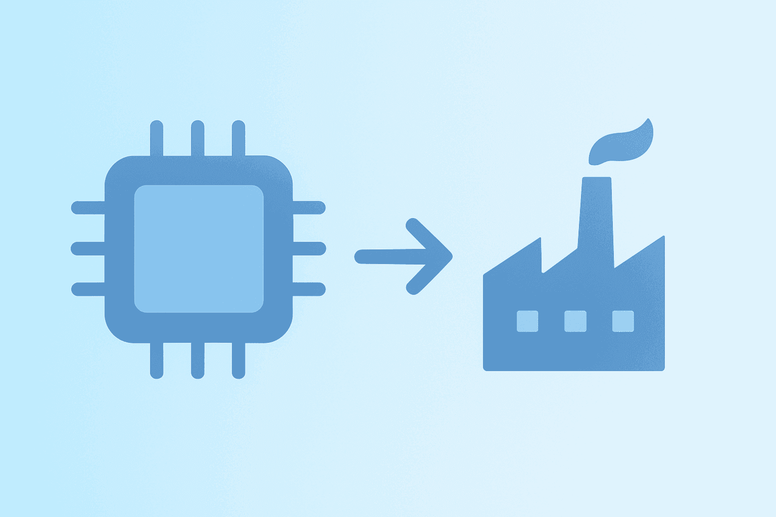
South Korea Semiconductor Investment Fuels Chip Push
South Korea semiconductor investment links a national chip and AI plan to Honam fab commitments, shifting memory supply assumptions and trader positioning.
KEY TAKEAWAYS
- Government unveiled an 800 trillion won Honam semiconductor hub with four new fabs.
- Samsung Electronics and SK Hynix will each build two fabrication plants.
- Policy aims to double DRAM output within five years and accelerate permitting.
HIGH POTENTIAL TRADES SENT DIRECTLY TO YOUR INBOX
Add your email to receive our free daily newsletter. No spam, unsubscribe anytime.
South Korea semiconductor investment was announced on June 29, 2026, when the government unveiled a national strategy pairing a new Honam chip-fab ecosystem with accelerated permitting and plans for Samsung Electronics and SK Hynix to expand domestic fabrication capacity to support AI infrastructure.
National Strategy and Goals
The government outlined a national industrial strategy centered on three “mega projects”: semiconductors, physical AI (robotics and hardware), and AI data centers. Officials framed the initiative as essential to securing core AI capabilities faster than other nations and promoting balanced regional growth beyond the Seoul metropolitan area. President Lee Jae Myung emphasized urgency, saying, “Speed is the only path to survival. We must secure the core elements of AI faster than any other nation.”
Science Minister Bae Kyung-hoon detailed an AI data center investment plan targeting 550 trillion won by 2029 and a total of about 1,000 trillion won by 2035, with roughly 10 gigawatts of added capacity. The government projects global AI data center investment could reach about US$5.5 trillion by 2030, creating strong demand for DRAM, NAND, and advanced packaging.
Industry Minister Kim Jung-kwan said the administration will accelerate construction and pre-secure scale to meet rising demand, aiming to double DRAM output within five years by advancing fab projects in the Seoul metropolitan area. The strategy seeks to maintain “overwhelming market leadership” and a decisive technological gap in memory semiconductors, focusing on high-bandwidth memory and advanced packaging critical for AI accelerators.
Honam Semiconductor Hub and Corporate Expansions
At the core of the plan is an 800 trillion won semiconductor ecosystem in the southwest Honam region, centered on Gwangju and South Jeolla. This area is designated as a second semiconductor production hub outside the existing Yongin and Pyeongtaek clusters. Industry Minister Kim said the project will include four fabrication plants, with Samsung Electronics and SK Hynix each building two. Samsung has selected Gwangju as its site, while SK Hynix is finalizing its southwest location.
Local governments in Gwangju and South Jeolla pledged 5–20 trillion won to complement corporate spending. The administration expects an 81 trillion won chip-packaging cluster in Chungcheong to complement the new fabs. Separate reports indicate Samsung is preparing a roughly 1,000 trillion won, decade-long investment plan spanning semiconductors, AI data centers, advanced packaging, and other units. Some accounts suggest combined Samsung and SK Hynix investments could reach as high as 2,000 trillion won over ten years, though these figures may overlap across categories.
Officials described the program as still in the policy announcement and strategic planning stage, with companies and regional authorities working to resolve land, power, water, and talent issues before full execution. President Lee highlighted Honam’s underused power and industrial water resources, citing technical assessments that the region could supply up to 1 million tons of industrial water per day to support large fabs. SK Hynix’s chairman noted the company needs more time to finalize a site and secure infrastructure.
If realized, the package would position South Korean memory makers as primary suppliers for AI infrastructure components and could reshape long-term market fundamentals for memory suppliers. The government set 2029 and 2035 as near- and medium-term benchmarks for data center and capacity build-outs, testing the expedited permitting push and companies’ ability to complete fabs and operating data centers.
AI Data Center Investment and Capacity Targets
Science Minister Bae Kyung-hoon outlined a plan to invest 550 trillion won in AI data centers by 2029, with a total program reaching about 1,000 trillion won by 2035. This includes adding roughly 10 gigawatts of AI data center capacity, bringing total capacity to about 18.4 gigawatts. The government views this build-out as a key demand corridor for memory chips and advanced packaging as AI workloads expand globally.
Officials said permitting approvals and construction timelines will be dramatically shortened to accelerate production capacity. President Lee emphasized that the southwest region offers abundant, underused power and sufficient industrial water to support rapid fab construction. The government aims to double DRAM output within five years by advancing fab projects in existing clusters and new hubs.
Permitting and Infrastructure
Industry Minister Kim said permit approvals and construction timelines will be “dramatically shortened” to enable rapid expansion. Samsung’s choice of Gwangju as a fab site signals forthcoming local zoning and permitting actions, while SK Hynix continues coordinating site selection and infrastructure needs.
President Lee referenced technical simulations showing the southwest region can supply 1 million tons of industrial water daily, supporting large fabs. The Honam project aligns with efforts to narrow regional disparities and build high-value industrial clusters outside Seoul, assigning the southwest a central role in future AI-era chip production.
Market and Strategic Implications
The government’s strategy aims to maintain South Korea’s “overwhelming market leadership” and a decisive technological gap in memory semiconductors, particularly for AI applications. The large-scale investments in fabs, packaging, and AI data centers are designed to position South Korea as a core supplier in the global AI infrastructure build-out.
The scale of investment, equivalent to large fractions of South Korea’s GDP and government budget, reflects the country’s commitment to securing long-term leadership in semiconductor and AI technologies. The initiative will test the government’s ability to expedite permitting and the companies’ capacity to execute ambitious expansion plans amid global demand for AI-related infrastructure.